What this source is
The source dossier is a compilation dossier on boron arsenide (BAs), assembled from heterogeneous materials rather than written as a single article. It gathers:
- four YouTube video summaries (LaVand MEDIA, Rice University's Smalley-Curl Institute, ScienceHubNet, and a short clip);
- a Wikipedia excerpt on boron arsenide and boron subarsenide (B₁₂As₂);
- abstracts and links to peer-reviewed papers in Science, Physical Review Letters, Physical Review B, Nature Communications, Advanced Science, Applied Physics Letters, and Materials Today, plus a phys.org news item and an arXiv preprint;
- a research-group page from UC Santa Barbara on boron arsenide growth;
- a patent layer of roughly 25 numbered documents (CN, US, WO, KR) with verbatim abstracts.
This composite character matters for how the page should be read. Unlike most the source archive dossiers in this wiki — which are single-inventor, free-energy or over-unity claims (see David Hamel, T. Henry Moray, Hans Coler) — this dossier concerns mainstream, peer-reviewed semiconductor materials science. The core thermal-transport discussion draws on journal literature and measurement; the patent and promotional entries must still be assessed separately. The "claims vs. evidence" framing still applies, but the evidence base is of a different kind: it is published experiment and first-principles calculation, and the main tensions are internal to that literature (theory vs. measurement, patent claims vs. measured values, isotope-enrichment disagreement).
The dossier is a compilation, not an independent validation. Nothing in it reports a new measurement by the source archive; every quantitative figure is quoted from a paper, a patent, or a video summary.
What boron arsenide is
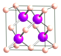
Boron arsenide is a III–V compound of boron and arsenic. The dossier's Wikipedia excerpt gives the basic properties of the cubic form (BAs) and of the subarsenide (B₁₂As₂):
| Property | BAs | B₁₂As₂ |
|---|---|---|
| Chemical formula | BAs | B₁₂As₂ |
| Molar mass | 85.733 g/mol | 279.58 g/mol |
| Appearance | Brown cubic crystals | — |
| Density | 5.22 g/cm³ | 3.56 g/cm³ |
| Melting point | 1,100 °C (decomposes) | — |
| Solubility in water | Insoluble | Insoluble |
| Band gap | 1.82 eV | 3.47 eV |
| Thermal conductivity | 1300 W/(m·K) (300 K) | — |
| Crystal structure | Cubic (sphalerite), cF8, No. 216 | Rhombohedral, hR42, No. 166 |
| Space group | F4̄3m | R3̄m |
| Lattice constant | a = 0.4777 nm | a = 0.6149 nm, c = 1.1914 nm; α=90°, β=90°, γ=120° |
| Formula units (Z) | 4 | 6 |
| CAS Number | 12005-70-8 | — |
Cubic BAs is a zinc blende (sphalerite) semiconductor with an indirect band gap of 1.82 eV and a lattice constant of 0.4777 nm. The dossier notes that chemical synthesis of cubic BAs is very challenging and that single crystals usually contain defects. It also reports that cubic BAs decomposes to the subarsenide B₁₂As₂ above 920 °C.
The subarsenide B₁₂As₂ is an icosahedral boride: a rhombohedral structure built from boron-atom clusters and two-atom As–As chains. It is a wide-bandgap semiconductor (3.47 eV) with a reported ability to "self-heal" radiation damage, can be grown on substrates such as silicon carbide, and has been proposed (though not currently used) for solar-cell fabrication.
A third form appears later in the dossier: hexagonal boron arsenide (h-BAs), synthesized as ultrathin nanosheets and used in memristors (see the Nature Communications 2025 item below).
The thermal-conductivity story
The scientific core of the dossier is the claim that cubic BAs conducts heat at rates approaching or rivaling diamond, and the decade-long effort to explain and measure it.
The 2013 prediction
The phys.org item (by Boston College) reports the first-principles prediction by David Broido (Boston College), Tom Reinecke (Naval Research Laboratory), and Lucas Lindsay (NRL postdoc). Conventional criteria — light, strongly bonded elements — predicted BAs should conduct heat about 10 times worse than diamond. Instead the calculation gave a room-temperature thermal conductivity above 2000 W/(m·K), exceeding diamond at higher temperatures.
The proposed mechanism: heat in an electrical insulator is carried by vibrational waves (phonons), and resistance comes from phonon–phonon collisions. In BAs, the team found an unusual interplay of vibrational properties in which the expected collisions are far less likely to occur in a certain frequency range, so large amounts of heat can be conducted there. This is the "phonon-band engineering" idea.
The 2018 measurements
The Science paper "Unusual high thermal conductivity in boron arsenide bulk crystals" (Fei Tian et al.) reports a local room-temperature thermal conductivity exceeding 1000 W/(m·K) and an average bulk value reaching 900 W/(m·K) in bulk BAs crystals. Its abstract states the result "departs from these long-held criteria" — that ultrahigh lattice thermal conductivity was thought possible only in crystals of strongly bonded light elements, limited by anharmonic three-phonon processes — and that the high values "can only be explained by higher-order phonon processes." The accompanying summary notes that three research groups (Kang et al., Li et al., and Tian et al.) independently synthesized high-purity BAs with conductivities around 1000 W/(m·K), roughly half that of diamond but more than double conventional metals.
The defect explanation
The Physical Review Letters paper "Antisite Pairs Suppress the Thermal Conductivity of BAs" (Qiang Zheng et al.) addresses why early measurements fell far short of the ~2000 W/(m·K) prediction. Using aberration-corrected scanning transmission electron microscopy (STEM), the authors looked for the As vacancies widely assumed to dominate thermal resistance — and did not find them. Instead they found enhanced intensity at some B columns and reduced intensity at some As columns, indicating antisite defects: As atoms on B sites (As_B) and B atoms on As sites (B_As). Calculation showed the As_B–B_As pair is energetically preferred among the point defects studied and lowers thermal conductivity. From an estimated antisite-pair concentration of 1.8(8)% (6.6±3.0×10²⁰ cm⁻³), the thermal conductivity was estimated at 65–100 W/(m·K), in reasonable agreement with the measured value. The paper concludes that As_B–B_As antisite pairs are the primary lattice defects suppressing thermal conductivity in BAs.
The four-phonon correction
The Physical Review B Rapid Communication "Four-phonon scattering significantly reduces intrinsic thermal conductivity of solids" (Tianli Feng, Lucas Lindsay, Xiulin Ruan) supplies the theoretical reconciliation. For decades only three-phonon scattering was considered; the authors show four-phonon scattering is generally important. For silicon and diamond it reduces predicted conductivity by 30% at 1000 K, bringing predictions into agreement with measurement. For zinc-blende BAs, four-phonon scattering is "strikingly strong" because three-phonon processes have an extremely limited phase space; it reduces the predicted room-temperature conductivity from 2200 to 1400 W/(m·K), and by 60% at 1000 K.
The value progression
The dossier presents a progression of measured values, but these come from different samples, methods, and groups — they are not a single reconciled number:
- 190 W/(m·K) — early measurements, attributed to high defect density;
- 900–1000 W/(m·K) — crystals with small defect density;
- 1300 W/(m·K) — high-quality crystals described in the source, reported as consistent with theory;
- ~1500 W/(m·K) — isotope-enriched c-¹¹BAs (2025).
The Wikipedia excerpt states the 1300 W/(m·K) figure is "the highest among all metals and semiconductors."
Isotope enrichment
The Advanced Science paper "Isotope-Enriched Cubic Boron Arsenide with Ultrahigh Thermal Conductivity" (Jaehoon Kim, Dongwook Lee, Huan Wu, et al.) reports synthesis of high-quality isotope-enriched c-¹⁰BAs and c-¹¹BAs crystals and a room-temperature thermal conductivity of 1500 W/(m·K) for c-¹¹BAs — described as the highest reported for isotope-enriched c-BAs.
The paper's introduction is candid about the prior state of the field. Because arsenic is a single isotope, the isotope effect in c-BAs is determined solely by boron (natural boron is 19% ¹⁰B, 81% ¹¹B, average mass 10.81). Previous isotope-enrichment studies had recorded "only minimal differences" in thermal conductivity between isotope-enriched and natural c-BAs, with most results in the 1100–1300 W/(m·K) range regardless of isotopic composition. The authors suggest those earlier results imply impurities had a more pronounced influence than isotope composition, and note that significant variations occur among crystals grown by identical methods, even within the same batch. Their own synthesis used a transition-metal catalyst and a modified chemical vapor deposition method; crystals were 100–400 µm, semi-transparent reddish, predominantly hexagonal or semi-hexagonal. Notably, the paper reports that measured values exceeded ab initio calculations.
Quantum phonon coherence
A 2026 Physical Review Letters item (Tong Lin et al., DOI 10.1103/qysd-d6rn) reports "Exceptional Optical Phonon Coherence in Enriched Cubic Boron Arsenide via Suppression of Three-Phonon Scattering." The Rice University video summary states that optical phonons in BAs can persist nearly 10 times longer than in typical materials. The abstract reports a record-high, isotope-purity-limited phonon coherence with a quality factor above 3.7×10³ for >98% enriched ¹¹BAs below 100 K, and that for the as-synthesized crystals defect scattering contributes negligibly to optical-phonon linewidth compared with isotope scattering. The work is attributed to Hanyu Zhu's group at Rice.
The semiconductor case
Beyond heat, the dossier argues BAs is a promising electronic material:
- Ambipolar mobility. BAs has high electron and hole mobility (>1000 cm²/V·s), unlike silicon, which has high electron mobility but low hole mobility. The UCSB growth page gives intrinsic values of 1,400 cm²/V·s (electron) and 2,110 cm²/V·s (hole). The Advanced Science paper cites a theoretically high hole mobility of 2100 cm²/V·s (versus silicon's 450, GaN's 40, GaAs's 400) and an experimentally confirmed ambipolar mobility of 1600 cm²/V·s.
- Band gap. 1.82 eV indirect.
- Thermal expansion compatibility. The arXiv preprint by Joon Sang Kang, Man Li, Huan Wu, Huuduy Nguyen, and Yongjie Hu reports systematic measurements: optical band gap 1.82 eV, refractive index 3.29 (657 nm), elastic modulus 326 GPa (twice silicon), and linear thermal expansion coefficient 3.85×10⁻⁶/K — close to GaN, which the authors note underscores BAs's promise for cooling high-power, high-frequency electronics.
- Thermal boundary conductance. A GaN-on-BAs structure exhibits a thermal boundary conductance (TBC) of 250 MW/m²·K, significantly higher than GaN-on-diamond.
- Integration. The Wikipedia excerpt states GaN–BAs heterostructures have been demonstrated with better performance than the best GaN HEMT devices on silicon carbide or diamond substrates, and that BAs composites have been developed as flexible thermal interfaces.
The dossier also notes a 2023 Nature study reporting that under high pressure BAs decreases its thermal conductivity — contrary to the typical increase seen in most materials.
The patent layer
The dossier's patent section lists roughly 25 documents with verbatim abstracts. They cluster into growth/synthesis, thermal management, and device applications.
| Patent | Title |
|---|---|
| CN121653852 | Boron arsenide indirect-direct band gap transformation method based on deep strain regulation and application |
| CN121183399 | Cosolvent for boron arsenide growth crystal, cubic boron arsenide crystal and synthesis method |
| CN120998370 | Method for calculating and regulating boron arsenide band gap based on first principle |
| CN120565503 | High-thermal-conductivity boron arsenide ceramic substrate and preparation method |
| CN120273026 | Production process of boron arsenide film crystal |
| US2025254902 | Semiconductor structure including high thermal conductivity material |
| WO2025072815 | Methods for high quality boron arsenide single crystal growth |
| KR102783297 | Boron arsenide of high thermal conductivity and synthesis method thereof |
| CN119194595 | Preparation method of boron arsenide film |
| CN118979307 | Equipment for preparing gallium arsenide single crystal (boron oxide / boron nitride crucible) |
| WO2024170071 | Device for producing an acoustic wave, and RF filter and multiplexer |
| US20260209990 | Structure comprising a high thermal conductivity boron arsenide layer |
| US2023257907 | Ultra-high ambipolar mobility cubic boron arsenide |
| CN116314350 | Boron arsenide resonant tunneling diode and manufacturing method |
| CN115666100 | Heat dissipation structure and power module assembly |
| CN115321552 | Boron arsenide nanocrystal synthesized by mechanochemical method |
| CN115259174 | Boron arsenide nanocrystal prepared from oxide |
| CN115196645 | Preparation method of boron arsenide powder |
| CN115208348 | Surface acoustic wave resonator, manufacturing method and filter |
| US2024055320 | Flexible thermal interface based on self-assembled boron arsenide |
| CN114105157 | Double-temperature-zone dense tube synthesis technology of boron arsenide powder material |
| US2021269318 | Unusual high thermal conductivity in boron arsenide bulk crystals |
| CN110137801 | Vertical cavity surface emitting laser and manufacturing method |
| US2021035885 | High thermal conductivity boron arsenide for thermal management, electronics, optoelectronics, photonics |
| KR20260077419 | Growth method for improving thermophysical property of isotope controlled high thermal conductivity boron arsenide |
Selected technical details from the abstracts:
- CN121653852 claims that applying 0.12 tensile strain along the [111] crystal orientation converts BAs from an indirect to a direct band gap, within the elastic limit, improving photoelectron transition efficiency.
- CN121183399 describes a low-pressure liquid-phase growth using an antimony–arsenic alloy melt as cosolvent, with a high-temperature end at 800–920 °C and a low-temperature end at 650–850 °C (at least 20 °C lower), slow cooling at ≤10 °C/h.
- CN120998370 uses VASP and vaspkit for modeling, static calculation, band calculation, and band-gap extraction under uniaxial strain.
- CN120273026 grows cubic BAs thin films on silicon by plasma-assisted deposition, carrying borane and arsine in argon and forming ionic arsenic and boron under a high-voltage arc.
- US2025254902 places BAs (thermal conductivity >1000 W/mK) as source/drain and/or heat spreader material in a stacked-channel semiconductor structure.
- WO2025072815 contacts elemental boron with elemental arsenic above arsenic's melting point, then separates liquid arsenic from the single-crystal product.
- US2023257907 claims c-BAs single crystals with room-temperature ambipolar mobility μ_a = 2μ_eμ_h/(μ_e + μ_h) greater than or equal to 1500, 1600, … up to 10000 cm²V⁻¹s⁻¹, with thermal conductivity ≥1000 Wm⁻¹K⁻¹.
- CN116314350 describes a BAs resonant tunneling diode with BAs barrier layers and a high-thermal-conductivity BAs single-crystal substrate, aimed at terahertz sources and digital logic.
- WO2024170071 and CN115208348 use c-BAs as a high-acoustic-velocity substrate in surface-acoustic-wave / RF filter devices.
- US2024055320 claims a thermal interface of a polymer composite with self-assembled boron arsenide.
- CN114105157 describes double-temperature-zone synthesis from 99.999% boron and arsenic in sealed quartz tubes (B:As molar ratio 1:1.5–1.9; high end 800–890 °C, low end 500–615 °C; 2–6 days), yielding cubic BAs powder of ≥99.995% purity.
- US2021269318 covers seeded chemical vapor transport (CVT) growth of bulk BAs crystals with controlled nucleation-center sparsity.
- CN110137801 uses graphene or boron arsenide as a heat-dissipation layer in a vertical cavity surface emitting laser.
Limitations, contradictions and unresolved questions
The dossier contains several internal tensions and apparent errors that should be flagged rather than resolved:
- Melting-point inconsistency. The Wikipedia excerpt's infobox gives a melting point of 1,100 °C (decomposes), while its prose states 2076 °C. Both appear in the same excerpt.
- Thermal-conductivity spread. Values of 190, 900–1000, 1300, and ~1500 W/(m·K) appear across the dossier. They come from different samples, methods, and groups and are not a single reconciled figure.
- Theory–experiment gap. First-principles predicted ~2200 W/(m·K) (three-phonon only), then ~1400 W/(m·K) (with four-phonon), then measurement gave ~1300 W/(m·K), then isotope-enriched samples gave ~1500 W/(m·K) — exceeding the ab initio prediction, as the Advanced Science paper itself notes.
- Sample quality and isotope effects. Prior studies found "only minimal differences" between isotope-enriched and natural c-BAs; the 2025 paper claims a clear improvement. Differences in sample quality and impurity scattering are relevant to this comparison; the values do not by themselves establish a direct contradiction.
- Patent claims vs. measured data. US2023257907 claims ambipolar mobility up to 10000 cm²/V·s, far above the ~1600 cm²/V·s experimentally confirmed elsewhere in the dossier. Patent claims are not evidence of achieved performance.
- CN115321552 abstract mismatch. The abstract text given for CN115321552 (boron arsenide nanocrystal by mechanochemical method) is a duplicate of CN115666100's heat-dissipation-structure text, not a nanocrystal-synthesis description — an apparent copy-paste error in the dossier.
- Video-summary assertions. The claim that BAs is "easier and cheaper to produce than diamond" and "doesn't require extreme temperatures or pressures" appears only in the ScienceHubNet video summary; the dossier provides no cost data. Treat as an assertion.
Related work and context
The dossier's scientific content connects to the broader literature on phonon transport and high-thermal-conductivity materials. Diamond (2200 W/m·K) and graphite are the reference points; the Advanced Science introduction notes diamond's high synthesis cost, chemical inertness, and slow growth rate, and graphite's anisotropic (low cross-plane) conductivity, as motivations for seeking alternatives. The four-phonon scattering work extends beyond BAs to silicon, diamond, thermoelectrics, thermal barrier coatings, nuclear materials, and radiative heat transfer.
Within this wiki, this source is a notable contrast to the free-energy and over-unity dossiers already present (David Hamel, T. Henry Moray, Hans Coler, entities/john-w-hendershot). It belongs to the same the source archive corpus (sources/main-archive, sources/library-annex) and touches the concepts/chemistry, concepts/physics, and concepts/energy topic guides, but its evidence base is peer-reviewed measurement rather than inventor testimony.
Source notes & attribution
- Rex Research, "Boron Arsenide — Articles & Patents," https://rexresearch.com/BoronArsenide/BoronArsenide.html (retrieved 2026-09-17).
- Fei Tian et al., "Unusual high thermal conductivity in boron arsenide bulk crystals," Science , https://www.science.org/doi/10.1126/science.aat7932.
- Sheng Li et al., "High thermal conductivity in cubic boron arsenide crystals," Science , https://www.science.org/doi/10.1126/science.aat8982.
- Qiang Zheng et al., "Antisite Pairs Suppress the Thermal Conductivity of BAs," Physical Review Letters 121, 105901, https://journals.aps.org/prl/abstract/10.1103/PhysRevLett.121.105901.
- Tianli Feng, Lucas Lindsay, Xiulin Ruan, "Four-phonon scattering significantly reduces intrinsic thermal conductivity of solids," Physical Review B 96, 161201, https://journals.aps.org/prb/abstract/10.1103/PhysRevB.96.161201.
- Jaehoon Kim, Dongwook Lee, Huan Wu, et al., "Isotope-Enriched Cubic Boron Arsenide with Ultrahigh Thermal Conductivity," Advanced Science , https://advanced.onlinelibrary.wiley.com/doi/10.1002/advs.202502544.
- Tong Lin et al., "Exceptional Optical Phonon Coherence in Enriched Cubic Boron Arsenide via Suppression of Three-Phonon Scattering," Physical Review Letters 136, 116903 (2026), https://doi.org/10.1103/qysd-d6rn.
- Dongwook Lee, Jaehoon Kim, Joon Sang Kang, "Highly reproducible synthesis of boron arsenide with high thermal conductivity," Applied Physics Letters 124, 222201, https://pubs.aip.org/aip/apl/article/124/22/222201/3295458.
- Joon Sang Kang, Man Li, Huan Wu, Huuduy Nguyen, Yongjie Hu, "Basic Physical Properties of Cubic Boron Arsenide," arXiv:1911.11281, https://arxiv.org/abs/1911.11281.
- Zenghui Wu et al., "Synthesis of hexagonal boron arsenide nanosheets for low-power consumption flexible memristors," Nature Communications 16, 4755 (2025), https://www.nature.com/articles/s41467-025-60038-3.
- Boston College, "An unlikely competitor for diamond as the best thermal conductor," phys.org, https://phys.org/news/2013-07-competitor-diamond-thermal-conductor.html.
- UC Santa Barbara, "Boron Arsenide Growth," https://palmstrom.cnsi.ucsb.edu/research/boron-arsenide-growth.
- Wikipedia, "Boron arsenide" (excerpt as reproduced in the dossier).
- https://rexresearch.com/BoronArsenide/BoronArsenide.html